Seven-Segment LED Display Decoder Module
Post by Souleymane Dembele on Aug 28, 2022
 According to Wikipedia,"A seven-segment display is a form of electronic
display device for displaying decimal numerals that is an alternative to the more complex dot matrix displays."
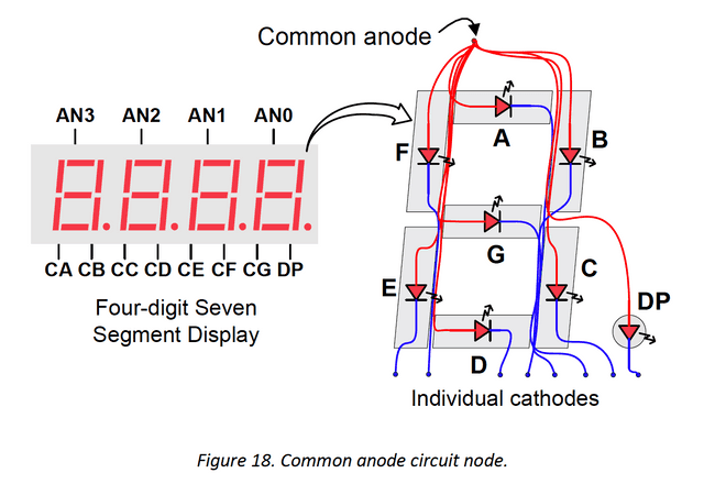
The Basys 3 prototyping board includes one four-digit common anode (CA) seven-segment LED display.

In fact, 7-segment LED displays are classified into two types:
- Common cathode (CC) and
- Common anode (CA).
The distinction between the two displays is that the common cathode connects all of the cathodes of the seven segments directly together, whereas the common anode connects all of the anodes of the seven segments together.
Each segment of the one the seven-segment display has an LED within. Since each LEDs may illuminate individually, we can have up to 128 possible patterns. To illuminate a segment, the anode should be driven high while the cathode is driven low. However, since the Basys 3 uses transistors to drive enough current into the common anode point, the anode enables are inverted. Therefore, both the AN0 up to AN3 and the CA up to CG/DP signals are driven low when active.
In our example, we will not be using DP signal (dot signal). However, we could use it perhaps when we are going through our multiplexer example where we will use AN0 through AN3; but at this time we will also use AN0 only for display/ decoding hexadecimal.
Hexadecimal to Seven-Segment (7-Segment) LED Display Module with Verilog
Hexadecimal is a base-16 numeral system. In contrast to our typical base 10 or binary systems, it may be utilized to express huge numbers with fewer digits. Hexadecimal comprises 16 symbols or numeric values ranging from 0 to 9, which are followed by six alphabetic characters: a, b, c, d, e, and f. Uppercase can be used as well. We will be repesenting lowercase.
The LED control signals a, b, c, d, e, f, and g are combined into a single 7-bit signal called seg. Since all hexadecimal digits can be comprised of a for-bit,
our module would take a four-bit as input and output a 7-bit for our prototyping board. Again depending on how the .xdc file is routed, the following would be our hexadecimal to 7-Segment module.
verilog1// a, b, c, d, e, f, g2// a3// ----4// f| g |b5// ----6//e| d |c7// ----8module hex_to_sseg(9 input wire [3:0] hex,10 output reg [6:0] seg11 );12 13always@(*)14begin15 case(hex)16 4'h0: seg[6:0] = 7'b0000001; // 4'h017 4'h1: seg[6:0] = 7'b1001111; // 4'h118 4'h2: seg[6:0] = 7'b0010010; // 4'h219 4'h3: seg[6:0] = 7'b0000110; // 4'h320 4'h4: seg[6:0] = 7'b1001100; // 4'h421 4'h5: seg[6:0] = 7'b0100100; // 4'h522 4'h6: seg[6:0] = 7'b0100000; // 4'h623 4'h7: seg[6:0] = 7'b0001111; // 4'h724 4'h8: seg[6:0] = 7'b0000000; // 4'h825 4'h9: seg[6:0] = 7'b0000100; // 4'h926 4'ha: seg[6:0] = 7'b0000010; // 4'ha27 4'hb: seg[6:0] = 7'b1100000; // 4'hb28 4'hc: seg[6:0] = 7'b0110001; // 4'hc29 4'hd: seg[6:0] = 7'b1000010; // 4'hd30 4'he: seg[6:0] = 7'b0010000; // 4'he31 default: seg[6:0] = 7'b0111000; // default 4'hf32 endcase33end34 35endmodule
We will also need our top module called
verilog1module top_hex_to_sseg(2 input clk,3 input [7:0] sw,4 output [3:0] an,5 output [6:0] seg6 );7 8assign an = 4'b1110;9 10hex_to_sseg sseg0(.hex(sw[3:0]), .seg(seg));11 12endmodule
To conclude, let's make sure to activate seven segments and our clock signal. Since we are using Switches for our for bit hex code we activated Switches as well.
xdc1## This file is a general .xdc for the Basys3 rev B board2 3# Clock signal4set_property PACKAGE_PIN W5 [get_ports clk]5 set_property IOSTANDARD LVCMOS33 [get_ports clk]6 create_clock -add -name sys_clk_pin -period 10.00 -waveform {0 5} [get_ports clk]7 8# Switches9set_property PACKAGE_PIN V17 [get_ports {sw[0]}]10 set_property IOSTANDARD LVCMOS33 [get_ports {sw[0]}]11set_property PACKAGE_PIN V16 [get_ports {sw[1]}]12 set_property IOSTANDARD LVCMOS33 [get_ports {sw[1]}]13set_property PACKAGE_PIN W16 [get_ports {sw[2]}]14 set_property IOSTANDARD LVCMOS33 [get_ports {sw[2]}]15set_property PACKAGE_PIN W17 [get_ports {sw[3]}]16 set_property IOSTANDARD LVCMOS33 [get_ports {sw[3]}]17set_property PACKAGE_PIN W15 [get_ports {sw[4]}]18 set_property IOSTANDARD LVCMOS33 [get_ports {sw[4]}]19set_property PACKAGE_PIN V15 [get_ports {sw[5]}]20 set_property IOSTANDARD LVCMOS33 [get_ports {sw[5]}]21set_property PACKAGE_PIN W14 [get_ports {sw[6]}]22 set_property IOSTANDARD LVCMOS33 [get_ports {sw[6]}]23set_property PACKAGE_PIN W13 [get_ports {sw[7]}]24 set_property IOSTANDARD LVCMOS33 [get_ports {sw[7]}]25 26#7 segment display27set_property PACKAGE_PIN W7 [get_ports {seg[6]}]28 set_property IOSTANDARD LVCMOS33 [get_ports {seg[6]}]29set_property PACKAGE_PIN W6 [get_ports {seg[5]}]30 set_property IOSTANDARD LVCMOS33 [get_ports {seg[5]}]31set_property PACKAGE_PIN U8 [get_ports {seg[4]}]32 set_property IOSTANDARD LVCMOS33 [get_ports {seg[4]}]33set_property PACKAGE_PIN V8 [get_ports {seg[3]}]34 set_property IOSTANDARD LVCMOS33 [get_ports {seg[3]}]35set_property PACKAGE_PIN U5 [get_ports {seg[2]}]36 set_property IOSTANDARD LVCMOS33 [get_ports {seg[2]}]37set_property PACKAGE_PIN V5 [get_ports {seg[1]}]38 set_property IOSTANDARD LVCMOS33 [get_ports {seg[1]}]39set_property PACKAGE_PIN U7 [get_ports {seg[0]}]40 set_property IOSTANDARD LVCMOS33 [get_ports {seg[0]}]41 42#set_property PACKAGE_PIN V7 [get_ports dp]43# set_property IOSTANDARD LVCMOS33 [get_ports dp]44 45set_property PACKAGE_PIN U2 [get_ports {an[0]}]46 set_property IOSTANDARD LVCMOS33 [get_ports {an[0]}]47set_property PACKAGE_PIN U4 [get_ports {an[1]}]48 set_property IOSTANDARD LVCMOS33 [get_ports {an[1]}]49set_property PACKAGE_PIN V4 [get_ports {an[2]}]50 set_property IOSTANDARD LVCMOS33 [get_ports {an[2]}]51set_property PACKAGE_PIN W4 [get_ports {an[3]}]52 set_property IOSTANDARD LVCMOS33 [get_ports {an[3]}]
Displaying digit (2)
